4th August 2019 – Added page.
23rd Oct 2019 – Added info


 Not an easy build and I made it harder. This panel requires a CGS 208 PCB, and a CGS 64 VCA PCB. Wiring diagram above is correct, note that I have added an extra VC DELAY input, and the switch on the VCA which allows for either VCA DELAY or a VCA on the input, these three amendments require additional resistors – see page above for wiring of these resistors. I put resistors in heatshrink and solder direct to the summing nodes. Check contacts on DPDT ON/ON/ON switch before proceeding, if different to switch noted above you will need to amend the switch wiring on the panel.
I have built a few WADs and IIRC all worked fine with values printed on PCB – apart from R21 which should be 820K, not 180K.
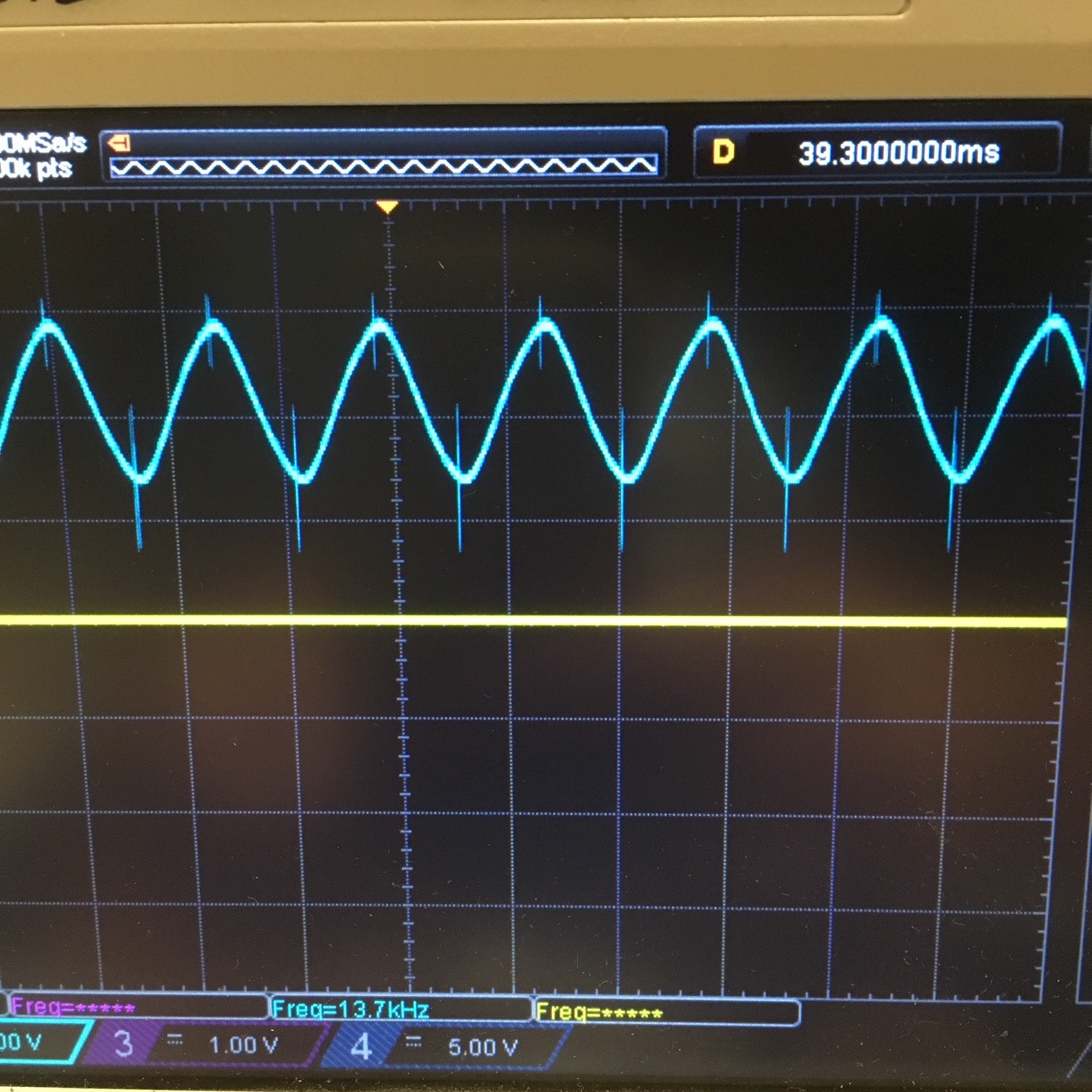
I may have to check this now there are more builders with these panels, so I’ll try and do some comparative tests etc. especially with regard to the values on the PCB vs Zthee’s values…
Here is a picture of Pin 1 U3 on my unit: