Avril 2022 – More CGS 514 stuff at bottom
12th August 2020 – scroll down for new CGS 514 info.
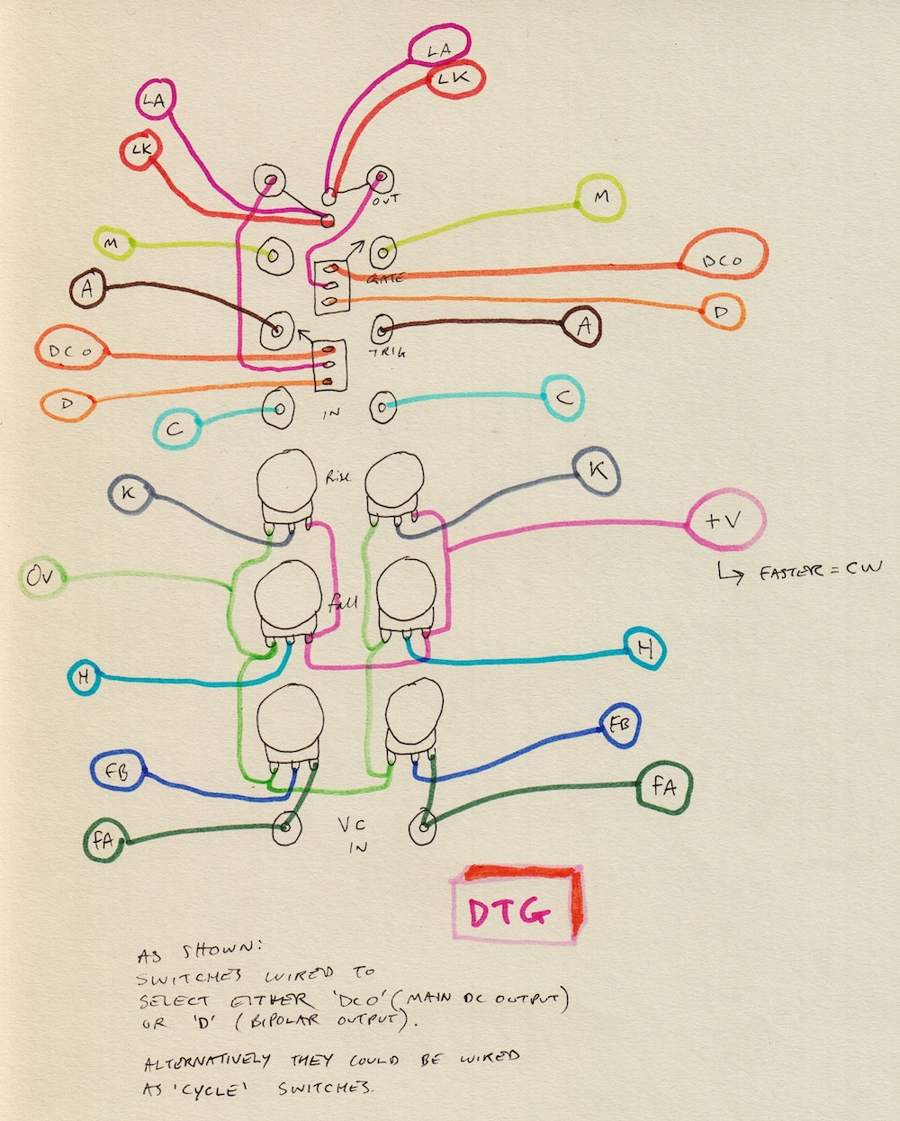
5th August 2019 – Added more information about possible modifications. Fixed some links. Added DTG wiring diagram.
4th August 2019 – Added 2″ DTG panel, scroll down past the DUSG info to see this, but worth reading build notes for both as it is the same PCB. The DUSG simply brings more controls to the panel.
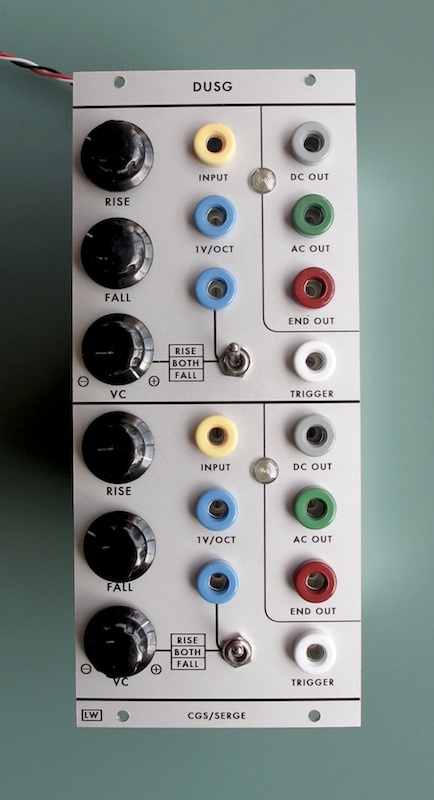
This following page details a possible means of construction for the CGS/Serge DUSG utilising the single function 4U panel from Loudest Warning.
More detailed information on the build is available here at Elby
The PCB’s (CGS 114) are available from Elby and Modular Addict
This panel utilises Clee’s 4U Bracket, which is available from Synthcube and Modular Addict
What is a DUSG? The DUSG has two independant USG’s, each of these consists of a positive slope generator (RISE) and a negative slope generator (FALL) combined to form one ‘universal slope generator’.
What can you do with the DUSG? It can be an AR generator, VC slew limiter, VC LFO, VCO, VC trigger delay, VC clock, VC low-pass filter, VC pulse divider and envelope follower. Further reading here.
Modifications
- For better audio rate operation replace the two 22NF capacitors with 10NF.
- For extended range on the RISE and FALL controls swap the 82K resistors connected topads H and K with 75K or even 68K. Personally I think 68K is too much range, but 75K works well.
- Remember to do the 100K / 1N trigger input replacement mod as detailed on Ken’s page, not doing this means unit may ‘lock up’ at audio rates.
- Replace the two chips marked LF353 on the PCB with OPA2134 for ‘better’ operation (especially in conjunction with the 10NF substitution mentioned above).
- Use high brightness (or super-bright) LEDs and use a higher value for the 1K LED resistor. I usually socket this resistor and swap different values in until I like the brightness. Using a low-current LED can cause problems with the circuit, and interaction between modules.
- Use matched high gain transistors in the core for best operation. On the DTG the matching is not really necessary as the panel has no 1V/OCT input. Neither design has temperature compensation anyway so maybe you don’t care about this. I will later detail how to modify circuit for better tracking using a trimpot and a 1K Tempco resistor. (I use BC 550 / 560 C transistors).
PLEASE NOTE – as drawn in this wiring diagram pots act CW = slower/longer Rise/Fall times. Reverse if you prefer the opposite direction. MA and MB are swapped, this message will disappear when I’ve redrawn the diagram.
Connection diagram for the LW DUSG panel, note that for the sake of clarity only half the connections are shown, hopefully it makes sense!

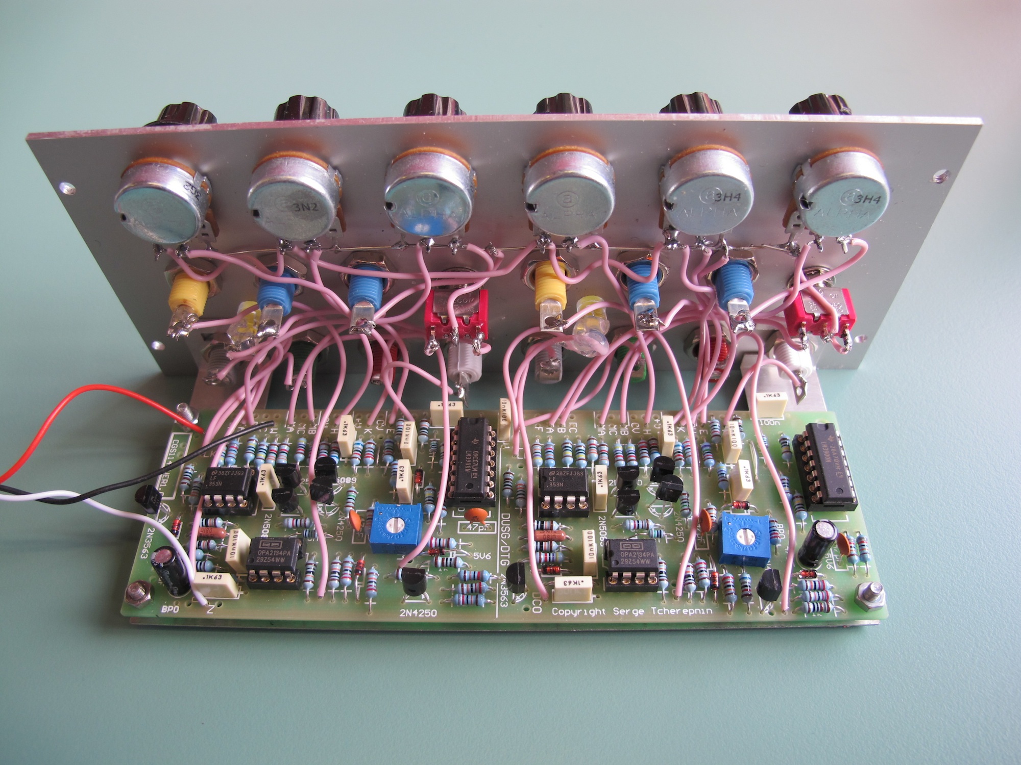
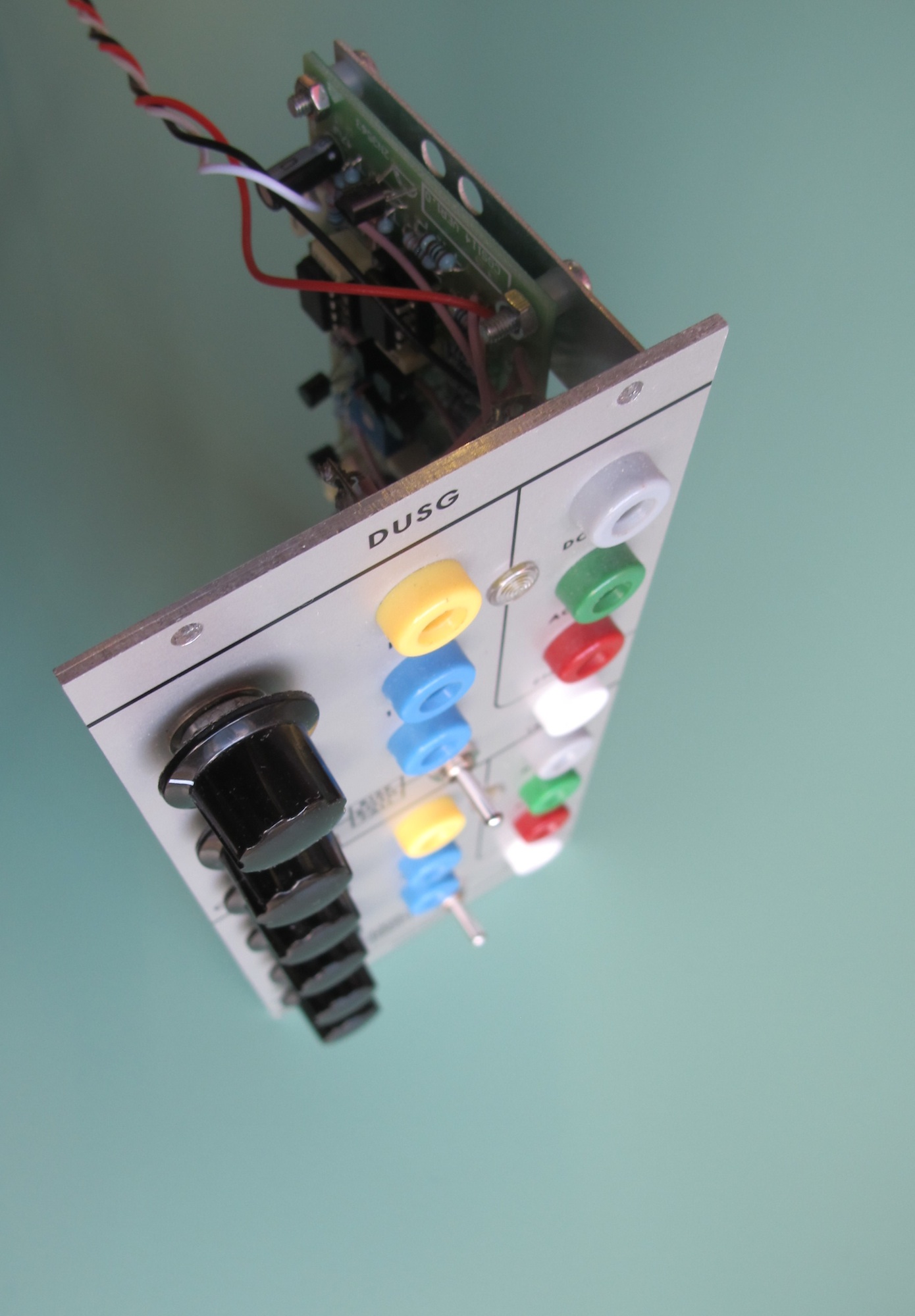
Here are some pictures of a completed build.


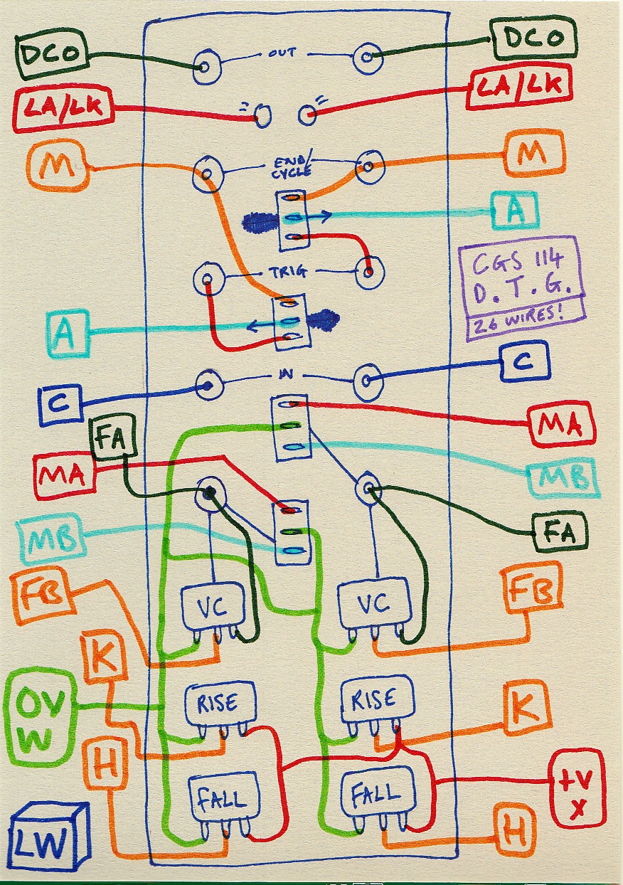
 Connection diagram for older DTG panel:
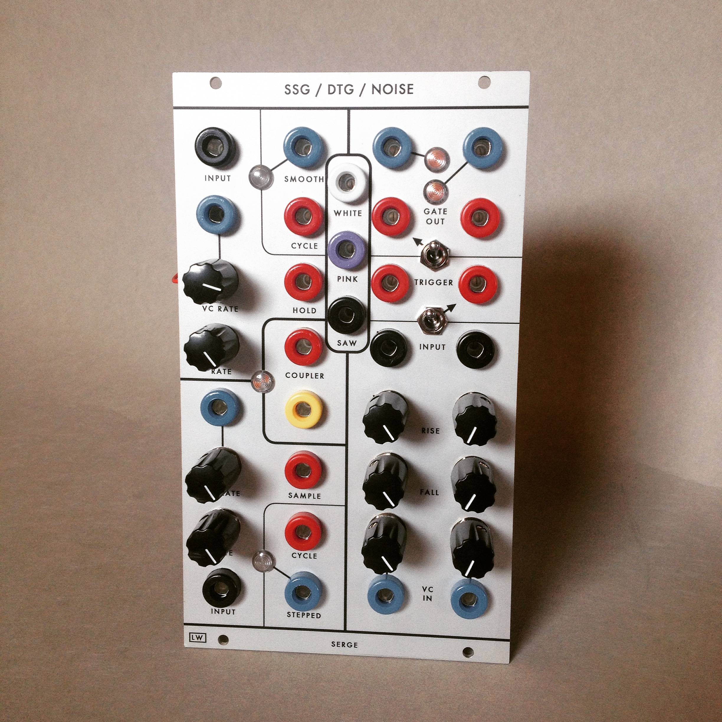
 OLD SSG / Noise / DTG panel:
New DTG panel build info:


 The picture below shows approximate wire lengths and how to mount bracket and PCB, with respect to the A and B slope generators:
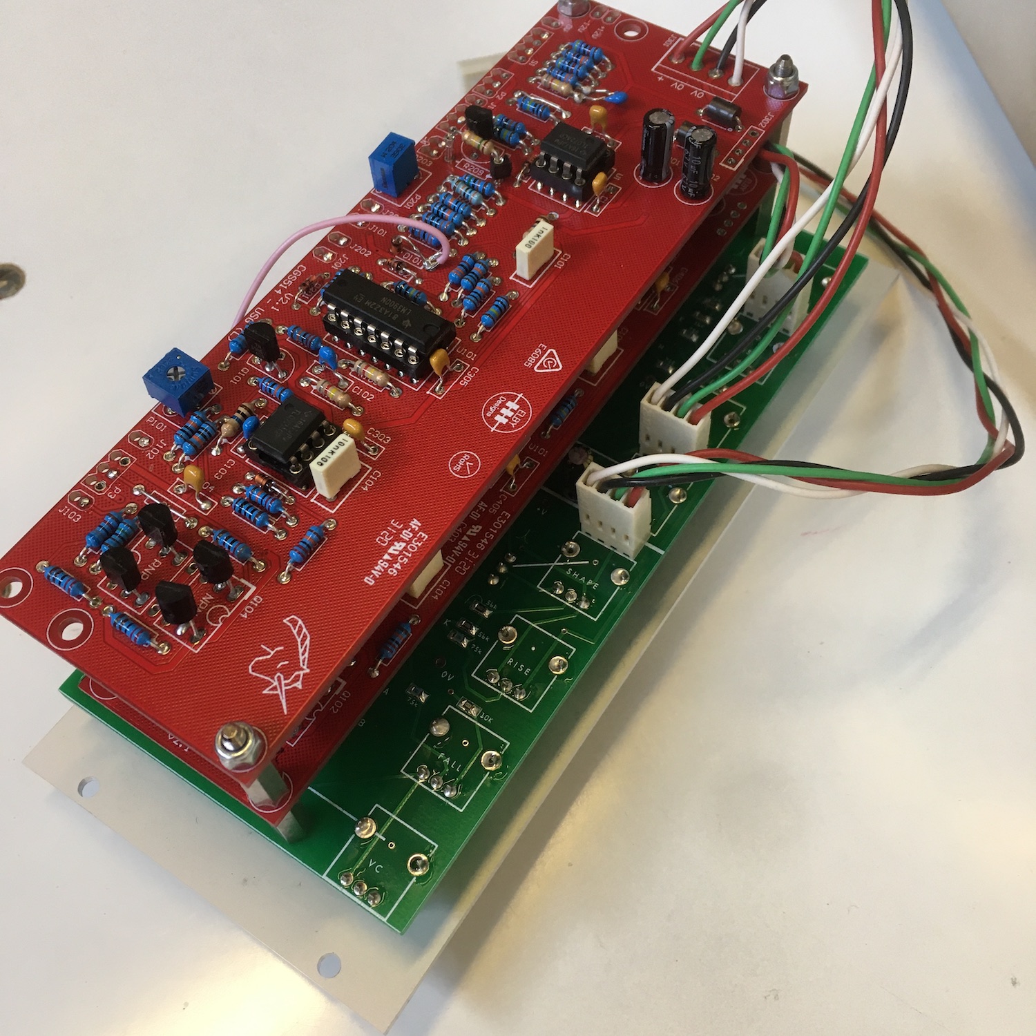
 CGS 514
New PCB!

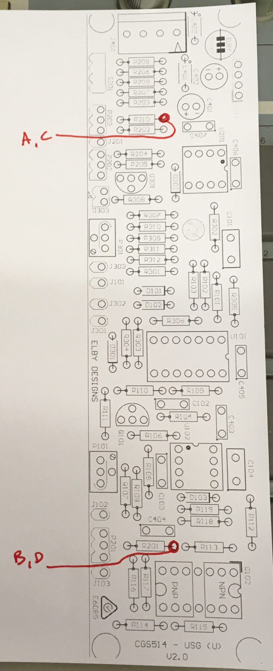
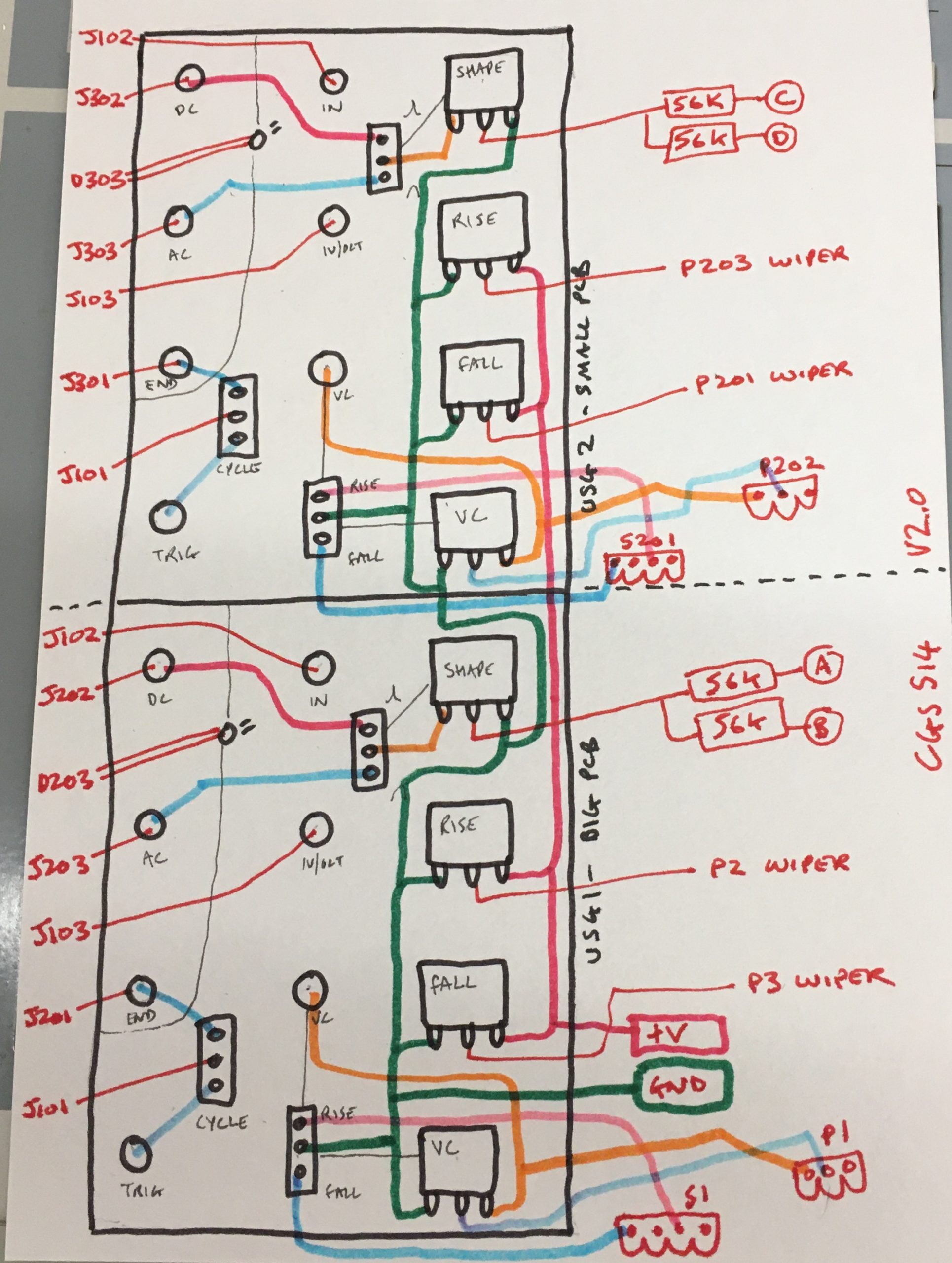 The SHAPE pot is wired (via 56K resistors) to these points on the PCB, basically after the RISE and FALL resistors, which are R1 and R10 on the lower (larger) PCB and R201 and R210 on the upper (smaller) PCB, shown here:
 I would suggest using 10NF rather than the specced 22NF cap – C104
PANEL PCB for CGS 514:
Some info on the panel PCB, BOM:
Ignore the TS321’s and two 0805 pads below it (see picture below)
10UF TH electrolytic x 2 (square pad with – symbol is -)
BC847 SMT x 4
56K 0805 x 4
75K 0805 x 4
10K 0805 x 4
100K 0805 x 2
LL4148 (SMT diode) x 2
100NF BP cap 0805 x 4
0.100″ headers, standoffs wire etc
8 x 50K LIN pots (Thonk vertical 9mm)
Banana jacks
4 x SPDT ON/ON switch
2 x SPDT ON/OFF/ON switch
For the switches I use these though there are others:
https://www.thonk.co.uk/shop/sub-mini-toggle-switches/
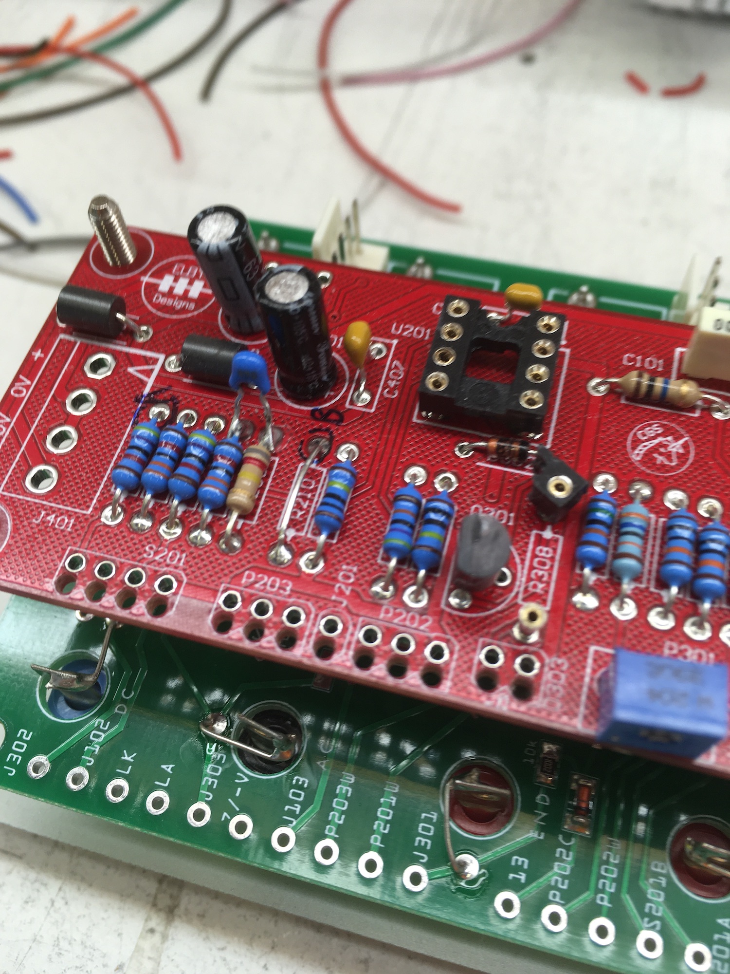
 On the 514 PCBs you need to jumper R1 and R10 on big PCB and R201 and R210 on the small PCB.
 Also it’s probably useful to mount D101 (both PCBs) like this:
 You will solder a wire from this point to the pad marked ’13’ on the panel PCB.
 Start with the smaller PCB – I use 15mm standoffs. Pads should be self-explantory, but P202W etc denotes ‘wiper’ – middle pad on the 514 PCBs. S1 and S201 / P1 and P202 pads are like this:

 I use the smaller PCB for the upper slope, see picture above for how ’13’ is soldered to the diode
 Each PCB has power from the panel PCB and thence to distro: